
DC COMPONENTS 1N4937 Инструкция по эксплуатации онлайн
Document Number: 88508 For technical questions within your region, please contact one of the following: www.vishay.com
Revision: 27-Oct-09 DiodesAmericas@vishay.com
, DiodesAsia@vishay.com, DiodesEurope@vishay.com 1
Fast Switching Plastic Rectifier
1N4933 thru 1N4937
Vishay General Semiconductor
FEATURES
• Fast switching for high efficiency
• Low forward voltage drop
• Low leakage current
• High forward surge capability
• Solder dip 275 °C max. 10 s, per JESD 22-B106
• Compliant to RoHS directive 2002/95/EC and in
accordance to WEEE 2002/96/EC
TYPICAL APPLICATIONS
For use in fast switching rectification of power supply,
inverters, converters and freewheeling diodes for consumer
and telecommunication.
Note
• These devices are not AEC-Q101 qualified.
MECHANICAL DATA
Case: DO-204AL, molded epoxy body
Molding compound meets UL 94 V-0 flammability rating
Base P/N-E3 - RoHS compliant, commercial grade
Terminals: Matte tin plated leads, solderable per
J-STD-002 and JESD 22-B102
E3 suffix meets JESD 201 class 1A whisker test
Polarity: Color band denotes cathode end
PRIMARY CHARACTERISTICS
I
F(AV)
1.0 A
V
RRM
50 V to 600 V
I
FSM
30 A
t
rr
200 ns
I
R
5.0 μA
V
F
1.2 V
T
J
max. 150 °C
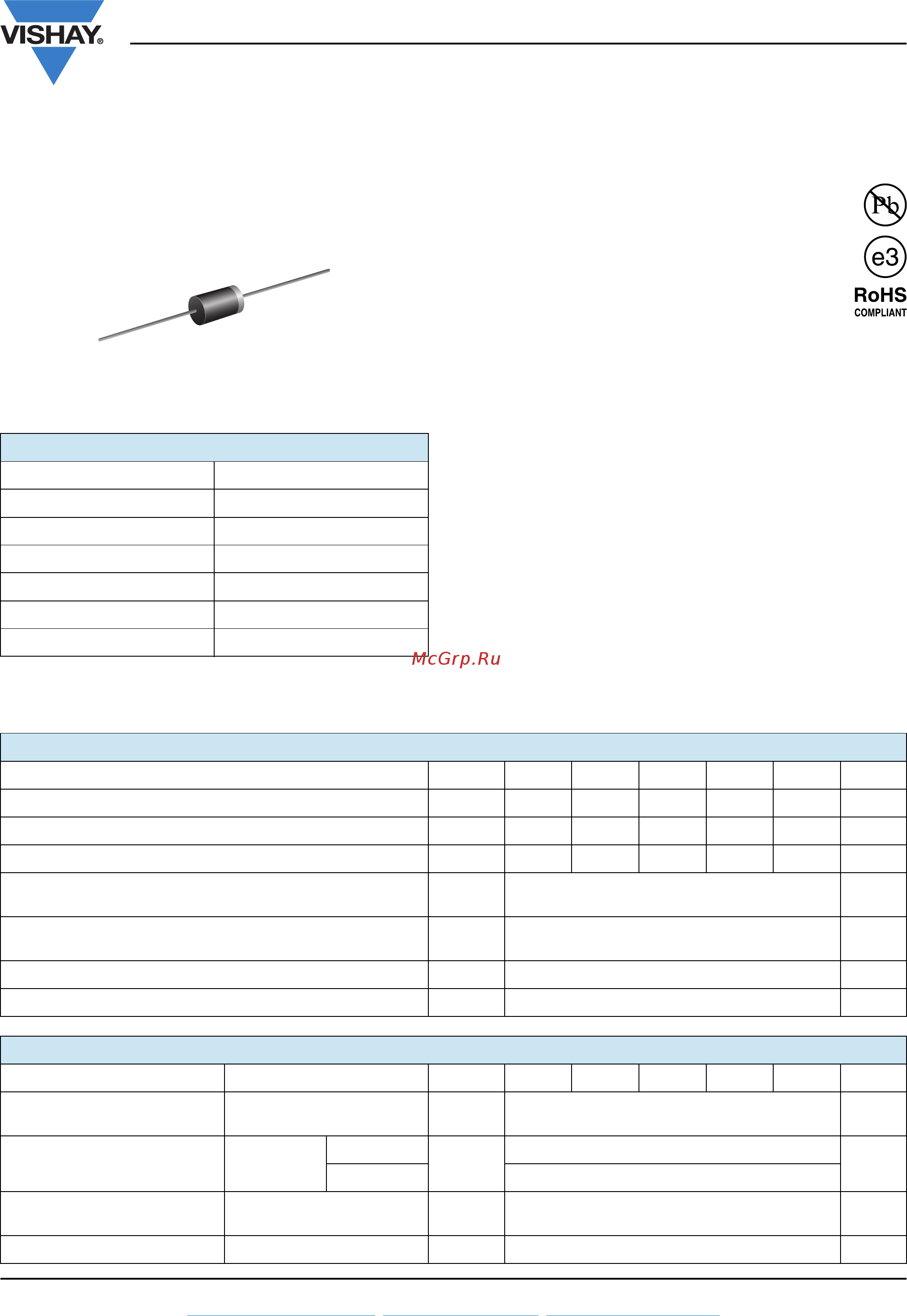
DO-204AL (DO-41)
MAXIMUM RATINGS (T
A
= 25 °C unless otherwise noted)
PARAMETER SYMBOL 1N4933 1N4934 1N4935 1N4936 1N4937 UNIT
Maximum repetitive peak reverse voltage V
RRM
50 100 200 400 600 V
Maximum RMS voltage V
RMS
35 70 145 280 420 V
Maximum DC blocking voltage V
DC
50 100 200 400 600 V
Maximum average forward rectified current
0.375" (9.5 mm) lead length at T
A
= 75 °C
I
F(AV)
1.0 A
Peak forward surge current 8.3 ms single half sine-wave
superimposed on rated load
I
FSM
30 A
Maximum reverse recovery current I
RM
2.0 A
Operating junction and storage temperature range T
J
, T
STG
- 50 to + 150 °C
ELECTRICAL CHARACTERISTICS (T
A
= 25 °C unless otherwise noted)
PARAMETER TEST CONDITIONS SYMBOL 1N4933 1N4934 1N4935 1N4936 1N4937 UNIT
Maximum instantaneous
forward voltage
1.0 A V
F
1.2 V
Maximum DC reverse current
at rated DC blocking voltage
T
A
= 25 °C
I
R
5.0
μA
T
A
= 100 °C 100
Maximum reverse recovery time
I
F
= 1.0 A, V
R
= 30 V,
dI/dt = 50 A/μs, I
rr
= 10 % I
RM
t
rr
200 ns
Typical junction capacitance 4.0 V, 1 MHz C
J
12 pF
Содержание
- 25 c unless otherwise noted 1
- Datasheet 1
- Electrical characteristics 1
- Fast switching plastic rectifier 1
- Features 1
- Maximum ratings 1
- Mechanical data 1
- N4933 thru 1n4937 1
- Primary characteristics 1
- Typical applications 1
- Vishay general semiconductor 1
- 25 c unless otherwise noted 2
- N4933 thru 1n4937 2
- Number of cycles at 60 hz 2
- Ordering information example 2
- Peak forward surge current a 2
- Ratings and characteristics curves 2
- Thermal characteristics 2
- Vishay general semiconductor 2
- 0 6 0 28 0 1 dia 3
- 2 0 80 2 dia 3
- 25 min 3
- 5 0 60 4 3
- N4933 thru 1n4937 3
- Package outline dimensions in inches millimeters 3
- Vishay general semiconductor 3
- Disclaimer 4
- Legal disclaimer notice 4
- Vishay 4
Похожие устройства
- DC COMPONENTS 1N4935 Инструкция по эксплуатации
- DC COMPONENTS 1N4934 Инструкция по эксплуатации
- DC COMPONENTS 1N4933 Инструкция по эксплуатации
- DC COMPONENTS 1N4448-DC Инструкция по эксплуатации
- DC COMPONENTS 1N4007A-DC Инструкция по эксплуатации
- DC COMPONENTS 1N4007-DC Инструкция по эксплуатации
- DC COMPONENTS 1N4005-DC Инструкция по эксплуатации
- DC COMPONENTS 1N4004-DC Инструкция по эксплуатации
- DC COMPONENTS 1N4003-DC Инструкция по эксплуатации
- DC COMPONENTS 1N4002-DC Инструкция по эксплуатации
- Sennheiser BT T100 Краткая инструкция
- Sennheiser BT T100 Инструкция
- Sennheiser AMBEO soundbar Инструкция
- Sennheiser AMBEO soundbar Краткая инструкция
- Sennheiser MOMENTUM Wireless Краткая инструкция
- Sennheiser MOMENTUM Wireless Инструкция
- Sennheiser PXC 550-II Wireless Инструкция
- Sennheiser PXC 550-II Wireless Краткая инструкция
- Калибр ДЭ-550/2ШМ Сборный чертеж
- Калибр ДЭ-550 ШМ Сборный чертеж